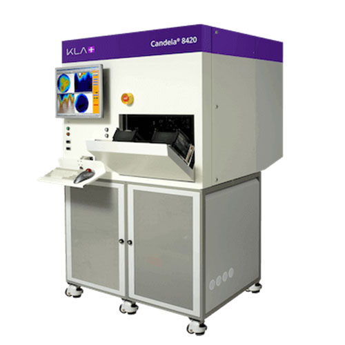
Candela® 8420 Surface Defect Inspection System
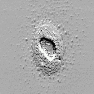
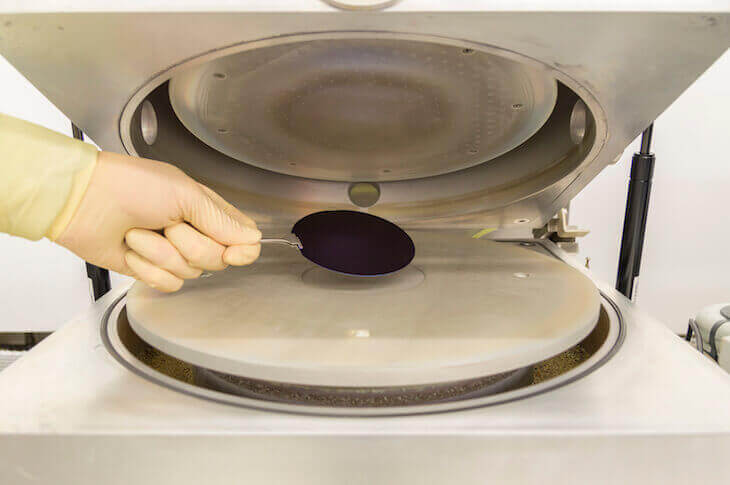
The Candela 8420 is a surface defect inspection system that uses multi-channel detection and rule-based defect binning to provide particle and scratch detection on opaque, translucent and transparent wafers such as Gallium Arsenide (GaAs), Indium Phosphide (InP), Lithium Tantalate, Lithium Niobate, glass, sapphire and other compound semiconductor materials. The 8420 surface defect inspection system employs proprietary OSA (optical surface analyzer) architecture to simultaneously measure scatter intensity, topographic variations, surface reflectivity and phase shift for automatic detection and classification of a broad range of defects of interest (DOI). Full-surface coverage is achieved in minutes, with the Candela 8420 surface defect inspection system to produce high resolution imaging and automated inspection reporting with defect classification and wafer maps.
The Candela 8420 wafer inspection system provides surface analysis including surface defect and particle detection on opaque, translucent and transparent wafers including glass, single side polished (SSP) sapphire, double side polished (DSP) sapphire; sliplines; Gallium Arsenide (GaAs) and Indium Phosphide (InP) pits and bumps; haze-like surface uniformity mapping; and defects on Lithium Tantalate (LiTaO2), Lithium Niobate (LiNbO3) and other advanced materials. The 8420 surface inspection system is used for compound semiconductor process control (wafer clean, pre- and post-epitaxy) using defect inspection. Its advanced multi-channel design offers improved sensitivity over single channel technologies. The CS20R configuration uses optics that are optimized to inspect compound semiconductor materials, including photosensitive films.


