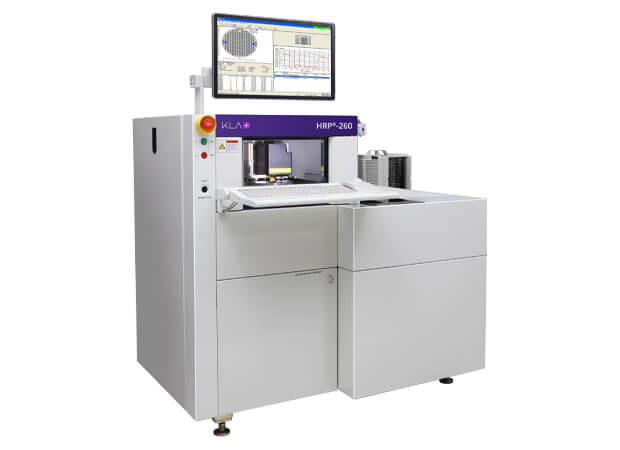
HRP®-260 Stylus Profiler
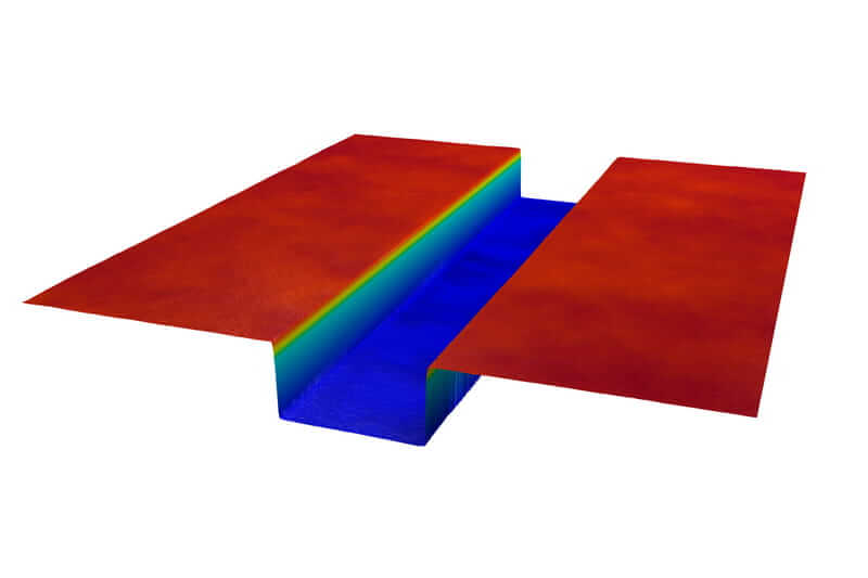
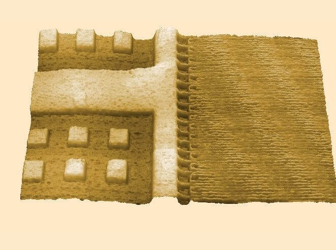
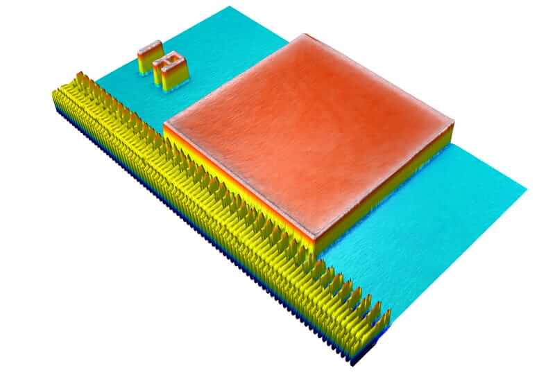
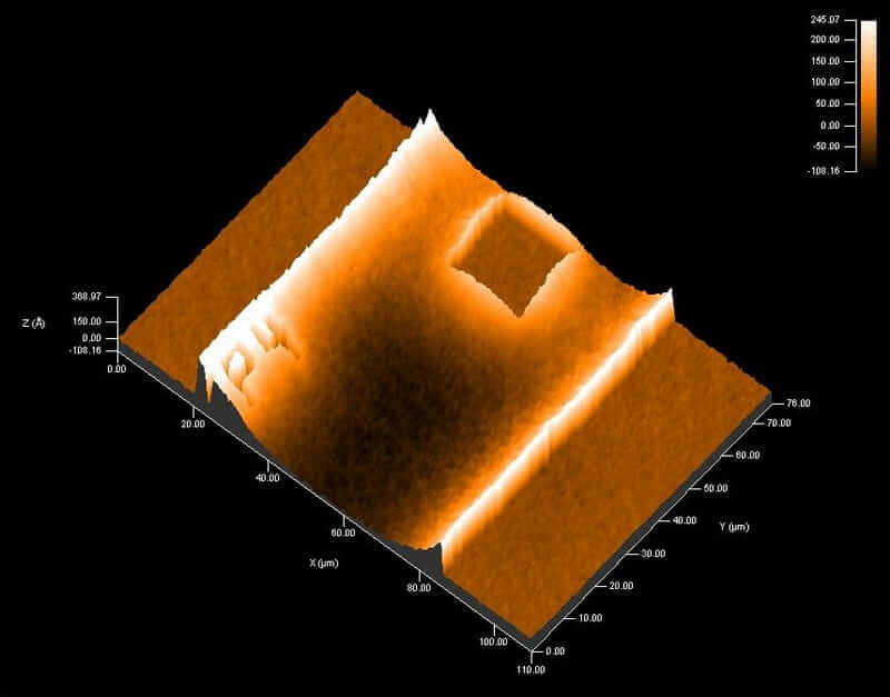
HRP®-260 is a high resolution, cassette-to-cassette stylus profiler offering step height measurement capability from a few nanometers to 300µm. The P-260 configuration supports 2D and 3D measurements of step heights, roughness, bow, and stress for scans up to 200mm without stitching. The HRP®-260 high resolution profiler configuration offers the same capability as the P-260, plus a high resolution stage that produces scanning results similar to an AFM. The high resolution profiler HRP platform has advanced pattern recognition algorithms that enhance recipe transportability between systems, a key requirement for a 24x7 production environments.
HRP®-260 high-resolution, cassette-to-cassette stylus profiler offers production proven performance with automated wafer handling capability serving the semiconductor, compound semiconductor, high brightness LED, data storage and related industries. The P-260 configuration supports 2D and 3D high-resolution measurements of step heights, roughness, bow, and stress for scans up to 200mm without stitching. The HRP®-260 configuration offers the same capability as the P-260, plus a high-resolution stage to measure small features at higher resolution and faster throughput.
HRP®-260 offers dual stage capability for measurement of nano- and micro-surface topography. The P-260 configuration offers long scan (up to 200mm) capability without stitching, and the HRP®-260 offers a high-resolution scanning stage for up to 90µm scan lengths. The P-260 achieves excellent measurement stability with a combination of the UltraLite®sensor, constant force control and ultra-flat scanning stage. The HRP®-260 enhances the capability with a high-resolution piezoelectric scanning stage. Recipe setup is fast and easy with point-and-click stage controls, low and high magnification optics, and high-resolution digital cameras. The HRP®-260 supports 2D and 3D surface measurement, with a variety of filtering, leveling, and data analysis algorithms to quantify the surface topography. Fully automated measurements are achieved with automated wafer handling, pattern recognition, sequencing and feature detection.


