Integrated Circuit (IC) Failure Analysis
Failure Analysis (FA) techniques are used to locate and identify the cause of failure in integrated circuits (IC).
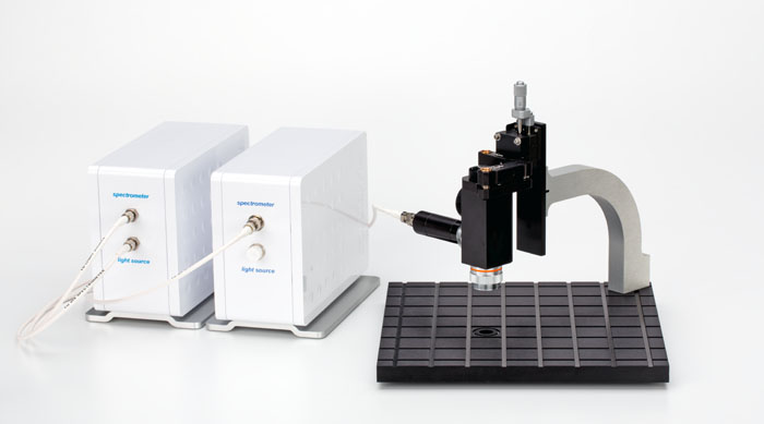
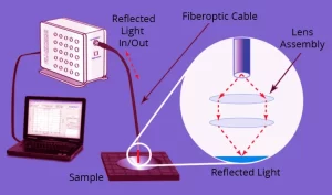
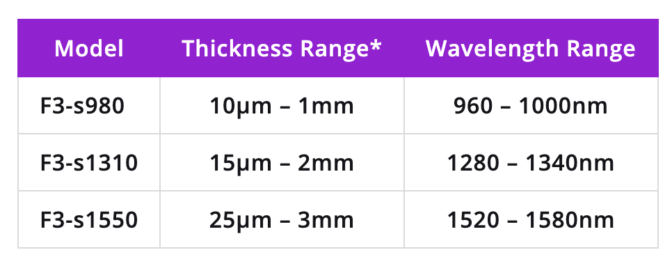
Backside thinning: Backside IC FA requires removing most of the Si die thickness before the circuitry can be imaged and knowing the thickness of the remaining Si after each thinning step. The Filmetrics F3-s1550 system was designed specifically for chip manufacturers to take on the challenge of measuring the thickness of rough Si layers resulting from various backside thinning processes.
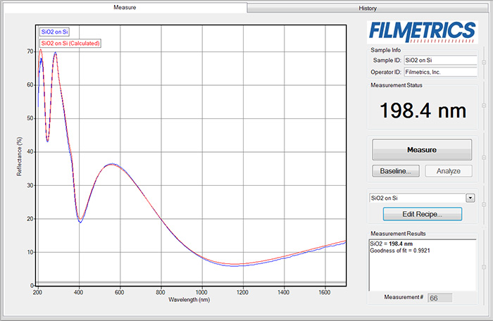
Photoresist Thickness Measurement
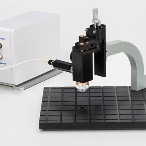
Several single-spot tabletop and mapping tools such as the Filmetrics F20, Filmetrics F3-sX and Filmetrics F50/F60-t measure photoresist thickness and etch rate of single-layer, multiple-layer and even freestanding photoresist films. All Filmetrics models measure resist thickness (and index) by accurately modeling spectral reflectance. Special proprietary algorithms allow robust “one-click” analysis, with results typically available in less than a second. Measurement of SU-8 thickness, Dow BCB thickness and other thick photoresists are popular applications for the Filmetrics product line.
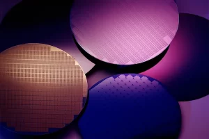
Silicon Wafer and Membrane Thickness Measurement
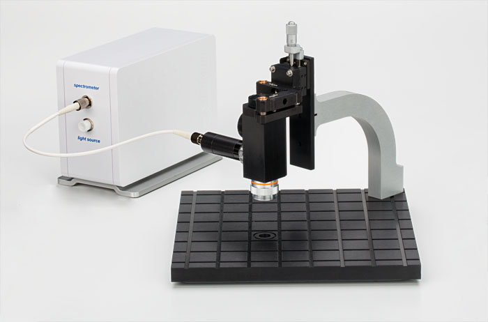
Filmetrics® systems include tabletop, mapping, and production systems for silicon wafer thickness measurement and membrane thickness measurement. Wafer materials commonly measured include single polished or double polished Si (Silicon), Sapphire, Fused Silica, SiC, LiTaO3, GaN, and Glass.
Our technical experts can help you find the best Filmetrics tool that fits your thickness measurement requirements that may include a need for various thickness ranges or a single-spot measurement vs. thickness mapping requirement, etc.