Zeta™-300 Optical Profiler

Zeta™-300 Optical Profiler

Zeta-300 optical profiler provides 3D metrology and imaging capability, combined with an integrated isolation table and configuration flexibility to handle larger samples. The 3D optical metrology system is powered by ZDot™ technology, which simultaneously collects high-resolution 3D data and a True Color infinite focus image. The Zeta-300 non-contact 3D profiler supports both R&D and production environments with Multi-Mode optics, easy-to-use software, and a low cost of ownership.


The Zeta-300 optical profiler is a non-contact, 3D surface topography measurement system. The Zeta-300 builds on the capability of the Zeta-20 3D profiler with additional isolation options and configuration flexibility to handle larger samples. The 3D optical metrology system is powered by patented ZDot technology and Multi-Mode optics, enabling measurement of a variety of samples: transparent and opaque, low to high reflectance, smooth to rough texture, and step heights from nanometers to millimeters.


The Zeta-300 optical profiler non-contact measurement system integrates six different optical metrology technologies in one configurable and easy-to-use system. ZDot measurement mode simultaneously collects a high-resolution 3D optical scan and a True Color infinite focus image. Other 3D optical metrology techniques include white light interferometry, phase shifting interferometry, Nomarski interference contrast microscopy, and shearing interferometry. Film thickness can be measured with ZDot or an integrated broadband reflectometer. The Zeta-300 is also a high-end microscope that can be used for sample review or automated defect inspection. The Zeta-300 3D profiler supports both R&D and production environments by providing comprehensive step height, roughness, and film thickness measurements and defect inspection capability.

Features

Easy to use optical profiler with ZDot and Multi-Mode optics to address a wide range of applications

High-quality microscope for sample review or defect inspection

ZDot: Simultaneously collects a high-resolution 3D scan and a True Color infinite focus image

ZI: Zeta phase and vertical scanning interferometry (PSI and VSI) enable wide area measurements with high z resolution

ZIC: Interference contrast for quantitative 3D data of surfaces with sub-nanometer roughness

ZSI: Shearing interferometry for images with high z resolution

images with high z resolution

ZFT: Film thickness and reflectance is measured with an integrated broadband reflectometer

AOI: Automatic optical inspection to quantify defects on the sample

Production capability: Fully automated measurements with sequencing and pattern recognition


Industries

LED: light emitting diodes and PSS (patterned sapphire substrates)

Semiconductor and compound semiconductor

Semiconductor WLCSP (wafer-level chip scale packaging)

Semiconductor FOWLP (fan-out wafer-level packaging)

PCB (printed circuit board) and flexible PCB

MEMS: Micro-electro-mechanical systems

Medical devices and microfluidic devices

Data storage

Universities, research labs and institutes

And more: Contact us with your requirements


Applications

Step height: 3D step height from nanometers to millimeters

Texture: 3D roughness and waviness on smooth to very rough surfaces

Form: 3D bow and shape

Stress: 2D thin film stress

Film thickness: transparent film thickness from 30nm to 100µm

Defect inspection: capture defects greater than 1µm

Defect review: KLARF files are used to navigate to defects to measure 3D surface topography or scribe defect locations


ZFT: Zeta Film Thickness

Zeta-300 可提供集成式宽频光谱仪,用于测量厚度30nm至100µm的透明薄膜。它能够测量单层或多层堆叠薄膜的厚度,用户从材料库中选择折射率值。可绘制样品上的薄膜厚度分布图,以确定样品的均匀性。

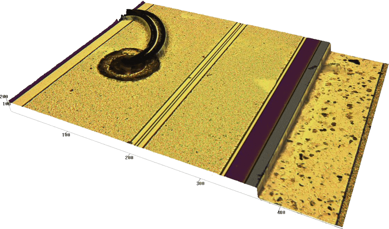
ZFT works on some of the least reflective surfaces, such as solar cells with reflectance of less than 0.1%. Many film thickness tools have difficulty obtaining a signal from these type of surfaces, since they depend on specular reflected light to calculate phase change or other parameters. The broadband white light and normal incidence illumination allow the tool to be used for a variety of optically transparent films with low reflectance.


ZI: Zeta Interferometry

The Zeta-300 supports phase scanning interferometry (PSI) and vertical scanning interferometry (VSI) when combined with the piezo stage and an interferometric objective lens. PSI enables fast measurements of step heights from angstroms to hundreds of nanometers. VSI, also known as white light interferometry (WLI), enables measurement of step heights from hundreds of nanometers to hundreds of microns. Both are performed at better than nanometer-level resolution, independent of the objective numerical aperture.

ZIC: Zeta Interference Contrast

The Zeta-300 utilizes Nomarski differential interference contrast microscopy to provide enhanced imaging of fine surface detail. Nomarski microscopy uses polarization and a prism to change the phase to enhance changes in slope on the sample surface. This enables visualization of defects on super-smooth surfaces, such as a monolayer of a contaminant. The ZIC scanning mode can convert these images into quantitative measurements of sub-nanometer level roughness by correlating the change in slope with roughness measured by another technique.

ZSI: Zeta Shearing Interferometer

The Zeta-300 shearing interferometer measurement technique (ZSI) enhances the ZIC measurement by adding a change in the phase. Multiple images are collected with different phases, then processed through advanced algorithms to generate a quantitative measure of surface topography with angstrom-level resolution. This technique does not require interferometric objectives and has no Z-stage scanning, resulting in high-resolution measurements from angstroms to 80nm.

Objective Lenses

The four-position turret holds objective lenses with magnifications ranging from 5X to 100X, to support nano-, micro- and macro-topography applications. The 5X objective is a Michelson interferometry objective. The 10X, 20X, 50X, and 100X objectives are Mirau interferometry objectives.

Couplers

The Zeta-300 can be configured with four different optical couplers to change the optics magnification. The system can be configured with the 1X coupler to keep the native magnification, or configured with 0.35X, 0.5X, or 0.63X couplers to increase the magnification.

Objective Lens Turret

The Zeta-300 can be configured with a 5 or 6 position manual turret and an objective lens sensor for automatic objective identification. The system can also be configured with a 5 or 6 position motorized turret for fully automated operation.

Sample Lighting

The Zeta-300 uses dual high-brightness white LEDs as standard lighting. Backlighting through the sample chuck is also available to enhance the light for challenging transparent samples, such as patterned sapphire substrates (PSS). The Zeta-300 also supports darkfield lighting from the side.

Stages

The Zeta-300 can be configured with a variety of stages to enhance system performance. A piezo Z-axis stage can be added to improve Z resolution for measurement of nanometer-level step heights with the ZDot or ZI measurement modes. An optional 280mm Z tower can accommodate large parts, such as tablets, phones and large machine components. The XY stage can be configured with a manual 300mm travel or motorized 150 or 200mm travel. A manual rotary stage can be added to the XY stage. A manual tip and tilt stage can be added to level the stage for interferometry measurements.


Sample Chucks

The Zeta-300 can provide stages that support various application requirements. Solar samples need to be paired with a 156mm sample stage or a solar tilt edge stage to tilt the sample and measure its edges. The backlit stage can be used for transparent substrates to support transmitted illumination. A 300mm wafer stage is available.

Isolation Tables

The system base of the Zeta-300 is equipped with built-in passive anti-vibration feet. For additional anti-vibration needs, passive or active benchtop anti-vibration platforms can also be provided.

Step Height and Film Thickness Standards

The Zeta-300 uses thin and thick film NIST traceable step height standards offered by VLSI Standards. The standards feature an etched quartz step with a chrome coating. A step height range of 8nm to 250µm is available.

An available certified multi-step standard has nominal step heights of 8, 25, 50, and 100µm. The standard has various pitch patterns for XY calibration. A certified film thickness standard is available for ZFT that includes a reference silicon surface and a nominal 270nm silicon dioxide film thickness. Reference roughness and mirror samples are also available.

Automated Sequencing Software

Automated sequencing software utilizes the motorized XY stage to allow the user to program measurement locations on the sample. The system will automatically measure each site and save the results in user-defined folders. An output report with sample statistics is generated to summarize the results.

Advanced sequencing software includes pattern recognition to automatically align the sample. This enables fully automated measurements, reducing the impact of operator error. Auto calibration can also be enabled when using embedded standards on the stage.

Stitching Software

Automated image stitching software utilizes the motorized XY stage to combine adjacent scans to generate a stitched data set that is larger than a single field of view. The system automatically measures every site, aligns the images, and combines them into one data set. The results can be analyzed like any other results file.

Apex Analysis Software

Apex analysis software enhances the tool’s standard data analysis capability with an extended suite of leveling, filtering, step height, roughness, and surface topography analysis techniques. Apex supports ISO roughness calculation methods plus local standards, such as ASME. Apex also serves as a report writing platform with the capability to add text, annotations, and pass/fail criteria. Apex is offered in eleven languages.

Offline Analysis Software

The Zeta-300 offline software has the same data analysis and program creation functions as the machine. This enables users to create programs and analyze data without occupying machine time.

Step Height

The Zeta-300 3D non-contact optical profiler is capable of measuring 3D, non-contact step heights from nanometers to millimeters. ZDot and Multi-Mode optics provide a range of methods to measure the step height. ZDot is the primary measurement technique and can quickly measure steps from tens of nanometers to millimeters. ZI interferometry can be used to measure steps from nanometers to millimeters over a large area. ZSI shearing interferometry can be used to measure steps less than 80nm.

Film Thickness

The Zeta-300 optical profiler is capable of measuring film thickness of transparent film(s) using ZDot or ZFT measurement techniques. ZDot is used to measure transparent films greater than 10µm, such as photoresist or microfluidic device layers that are coated on higher refractive index substrates. ZFT uses an integrated broadband reflectometer to measure films from 30nm to 100µm. This can be done for a single or multiple-layer film stack, with the user entering the properties of the film or using a model to fit the spectrum.


Texture: Roughness and Waviness

The Zeta-300 3D profiler measures 3D texture, quantifying the sample’s roughness and waviness. ZDot enables measurement of roughness ranging from tens of nanometers to very rough surfaces. ZSI and interferometry enable measurement of smooth surfaces, from angstroms to microns. Software filters separate the measurements into roughness and waviness components and calculate parameters, such as root mean square (RMS) roughness. Nomarski interference contrast microscopy enables visualizing very fine surface detail by revealing small changes in the slope.


Form: Bow and Shape

The Zeta-300 non-contact 3D profiler can measure the 2D and 3D shape or bow of a surface. This includes measurement of wafer bow that can result from mismatch between layers during the production of semiconductor or compound semiconductor devices. The Zeta-300 can also quantify the 3D height and radius of curvature of structures, such as a lens.


Stress: Thin Film Stress

The Zeta-300 is capable of measuring stress induced during the manufacture of devices with multiple layers, such as semiconductor or compound semiconductor devices. The bow of the surface is accurately measured using a stress chuck to support the sample in a neutral position. The change in shape from a process, such as film deposition, is then used to calculate the stress, applying the principles of Stoney’s equation. The Zeta-300 measures 2D stress by finding the height of the sample surface at user-defined intervals across the full sample diameter and then combining the data into a profile of the sample shape.

Automated Defect Inspection

The Zeta-300 is capable of Automated Optical Inspection (AOI) to rapidly inspect the sample, differentiate different defect types, and map defect density across the sample. When combined with the 3D metrology capability, the Zeta-300 can provide additional information about the defect that cannot be obtained with 2D inspection systems, enabling quicker identification of the defect source.

Defect Review

Zeta-300 defect review uses an inspection tool KLARF file to drive the stage to the defect locations. The user can inspect the defect with the high-quality microscope or measure the topography of the defect, such as the height, thickness, or texture. This provides additional detail about the defect that cannot be obtained from a 2D defect inspection system. The Zeta-300 can also mark defects with a scribe, making it easier to find the defect on tools, such as SEM review tools, that have a limited field of view.

LED Pattern Sapphire Substrates (PSS)

The Zeta-300 optical profiler supports metrology and inspection of patterned sapphire substrates. The system combines ZDot, through-sample lighting and custom algorithms to quickly quantify the height, width, and pitch of PSS bumps. The Zeta-300 can also be used to measure the photoresist before and after patterning, enabling sample rework before sapphire etch. Automated defect inspection of PSS substrates enables rapid identification of critical defects, such as missing PSS bumps, bump bridging, tear-out and contamination.

Semiconductor and Compound Semiconductor Packaging

The Zeta-300 supports Wafer-Level Chip Scale Packaging (WLCSP) and Fan-Out Wafer Level Packaging (FOWLP) metrology requirements. A key enabling technology is the capability to measure the height of the plated copper with the dry photoresist film intact. This is accomplished by measuring through the transparent photoresist to the seed layer to measure the height of the copper pillar, thickness of the photoresist, and relative height difference of copper and photoresist. Additional applications include measurement of redistribution lines (RDL), under bump metallization (UBM) height and texture, photoresist opening critical dimension (CD), photoresist thickness, and polyimide thickness. Coplanarity of the metal contacts can also be measured to determine if the bump height meets final device packaging connectivity requirements.

Printed Circuit Board (PCB) and Flexible PCB

The Zeta-300’s high dynamic range enables surface roughness and step height measurements from nanometers to millimeters without a configuration change. It can handle high-reflectance films (e.g., copper) as well as transparent films that are commonly found on PCBs. The Zeta-300 supports critical dimension measurements (height and width) for blind via holes, line traces and hot bars, plus surface roughness.

Laser Ablation

The Zeta-300 can measure topography changes induced by laser surface processing for semiconductors, LED, microfluidic devices, PCBs, and more. Lasers have been adopted for precision micro-scale machining and surface conditioning in industries, such as semiconductors, LED, and biomedical devices. For the semiconductor industry, measurement of the height and width of a wafer ID mark is critical to ensuring it can be read successfully throughout numerous processing steps.

Microfluidics

The Zeta-300 has the capability to measure microfluidic devices fabricated in materials, such as silicon, glass, and polymers. The system quantifies the height, width, edge profile, and texture of channels, wells, and control structures. The Zeta-300 can also measure the final device after it is sealed with a transparent top cover plate – compensating for the change in refractive index and quantifying changes from the stress of applying the cover plate.

Biotechnology

Zeta-300非常适合生物技术应用,可对具有从纳米级到毫米级特征的各种样品表面进行非接触式测量。Zeta-300可以测量高高宽比台阶,例如生物技术器件的深孔的深度。借助高数值孔径物镜和对反射能力极弱的样品的分辨能力,可以测量用于药物输送的微针阵列结构

related news

contact us

我们希望了解您的需求,请填写以下表单并提交

Your Name
邮箱地址
联系电话
您的需求