Tencor® P-170 Stylus Profiler

Tencor® P-170

The Tencor P-170 stylus profiler is a cassette-to-cassette profiler offering step height measurement capability for steps from a few nanometers to one millimeter, for production environments.


The profiler system supports 2D and 3D measurements of step heights,®roughness, bow, and stress for scans up to 200mm without stitching.


The Tencor P-170 has advanced pattern recognition algorithms,®enhanced optics, and an advanced stage for robust performance and seamless recipe transportability between systems – a key requirement for a 24x7 production environment.

Features

Step height: Nanometers to 1000µm

Low Force: 0.03 to 15mg

Scan full diameter of the sample without stitching

Video: 5MP high-resolution color camera

Arc Correction: Removes error due to arc motion of the stylus

Software: Easy-to-use software interface

Production capability: Fully automated with sequencing, pattern recognition and SECS/GEM

Wafer handler: Automatically loads 75mm through 200mm opaque (e.g., silicon) and transparent (e.g., sapphire) samples


Industries

Semiconductor

Compound semiconductor

LED: Light emitting diodes

MEMS: Micro-electro-mechanical systems

Data storage

Automotive

And more: Contact us with your requirements


Applications

Step Height: 2D and 3D step height

Texture: 2D and 3D roughness and waviness

Form: 2D bow and shape

Stress: 2D and 3D thin film stress

Defect review: 2D and 3D defect surface topography


Stylus Options

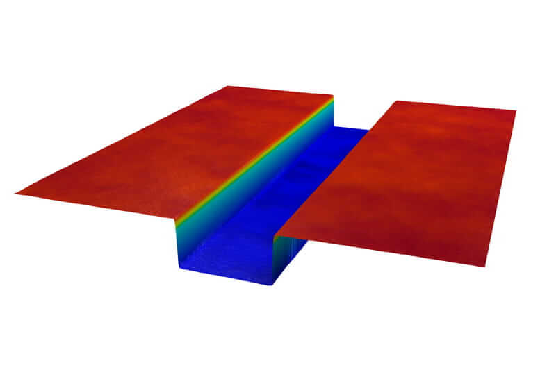
Tencor P-170提供多种探针用于测量台阶高度、台阶高宽比、粗糙度、样品翘曲度和应力。探针针尖的半径从40纳米到50微米不等,这决定了测量的横向分辨率。探针角度从20到100度不等,这决定了所测量特征的最大高宽比。所有探针都采用金刚石制造,以减少磨损并增加其使用寿命。


Sample Chucks

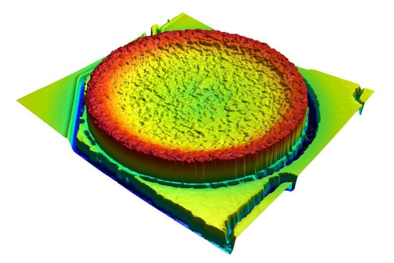
The Tencor P-170 has a range of chucks available to support application requirements. The standard is a vacuum chuck with support for measuring samples from 75 to 200mm. A stress chuck is available with 3-point locators to support the sample in a neutral position for accurate bow measurements. Additional options for bowed wafer sample handling are available.

Handler Options

The Tencor P-170 handler includes an aligner for opaque wafers (e.g., GaAs) and a cassette station for 200mm wafers. Options include transparent sample alignment (e.g., sapphire), smaller sample sizes ranging from 75mm to 150mm, a second cassette station, a cassette slot mapper, a signal tower, and an ionizer.

Isolation Tables

The Tencor P-170 is configured with the TMC 68-500 Series free-standing isolation table, which uses air isolators to provide passive isolation. This is a custom isolation table that meets SEMI S8 ergonomic requirements, placing the keyboard, mouse, monitor, and cassette station at the correct ergonomic height.


Step Height Standards

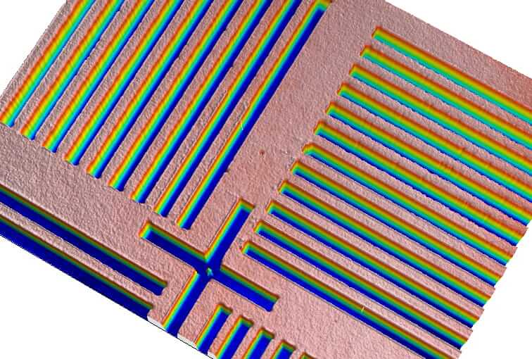
The Tencor P-170 uses thin and thick film NIST-traceable step height standards offered by VLSI Standards. The standards feature an oxide step on a silicon die mounted on a quartz block, or an etched quartz step with a chrome coating. 200mm wafer based step height standards are also available. A step height range of 8nm to 250µm is available.


Apex Analysis Software

Apex analysis software enhances the standard data analysis capability of the Tencor P-170 with an extended suite of leveling, filtering, step height, roughness, and surface topography analysis techniques. Apex supports ISO roughness calculation methods, plus local standards, such as ASME. Apex can also serve as a report writing platform with the capability to add text, annotations, and pass/fail criteria. Apex is offered in eleven languages.


Offline Analysis Software

The Tencor P-170 offline software has the same data analysis and recipe creation capability that exists on the tool. This enables the user to create recipes and analyze data without using valuable tool time.


Pattern Recognition

Pattern recognition uses pre-taught patterns to automatically align the sample. This enables fully automated measurements for enhanced measurement stability by reducing the impact of operator error. Pattern recognition combined with advanced calibrations reduces stage positioning error and enables seamless transfer of recipes between systems.


SECS/GEM and HSMS

SECS/GEM and HSMS communications support factory automation systems and enable remote control of the Tencor P-170. Measurements results are automatically reported to host SPC systems, plus alarms and key calibration/configuration data. The Tencor P-170 is compliant with SEMI standards E4, E5, E30, and E37.

Step Height

The Tencor P-170 is capable of measuring 2D and 3D step heights from nanometers to 1000µm. This enables quantification of material deposited or removed during etch, sputter, deposition, spin coating, CMP and other processes. The Tencor P-170 has constant force control that dynamically adjusts to apply the same force on the sample surface, regardless of step height. This results in good measurement stability and enables accurate measurement of soft materials, such as photoresist.


Texture: Roughness and Waviness

The Tencor P-170 measures 2D and 3D texture, quantifying the sample’s roughness and waviness. Software filters separate the measurement into the roughness and waviness components and calculate parameters, such as the root mean square (RMS) roughness.


Form: Bow and Shape

The Tencor P-170 can measure the 2D shape or bow of a surface. This includes measurement from wafer bow that can result from mismatch between layers during device fabrication, such as deposition of multiple layers for the production of semiconductor or compound semiconductor devices. The Tencor P-170 can also quantify the height and radius of curvature of structures, such as a lens.


Stress: 2D and 3D thin film stress

The Tencor P-170 is capable of measuring the stress induced during the manufacture of devices with multiple process layers, such as semiconductor or compound semiconductor devices. The bow of the sample is accurately measured using a stress chuck to support the sample in a neutral position. The change in shape from a process, such as film deposition, is then used to calculate the stress by applying Stoney’s equation. 2D stress is measured with a single scan across the sample diameter for samples up to 200mm without the need to stitch. 3D stress is measured using a combination of 2D scans, with the theta stage rotating between scans to measure the full sample surface.


Defect Review

Defect Review is used to measure the topography of defects, such as the depth of a scratch. Defect inspection tools identify defects and write the location coordinates to a KLARF file. The Defect Review feature reads the KLARF file, aligns the sample, and allows the user to select defects for 2D or 3D measurement.


related news

contact us

我们希望了解您的需求,请填写以下表单并提交

Your Name
邮箱地址
联系电话
您的需求