Nano Indenter® G200X Nanoindenter

Nano Indenter® G200X

The Nano Indenter G200X provides an easy-to-use nanoscale mechanical tester that quickly delivers accurate, quantitative results. The G200X nanoindenter system handles a wide variety of samples from hard coatings to soft polymers and offers the most comprehensive test suite available in the KLA Instruments nanoindenter product line. The new G200X Semi Pack offers advanced solutions for semiconductor and compound semiconductor films characterization.


The Nano Indenter G200X provides an easy-to-use nanoscale mechanical tester that quickly delivers accurate, quantitative results. The G200X system includes our highest performing motion system, largest sample mounting system and our high-resolution optical microscope. Our InView software, InQuest controller and InForce actuators deliver the same high performance results across the product line up. The G200X system options include the continuous stiffness measurement (CSM), scanning probe microscopy, scratch testing, frequency sweeps, electrical measurements, high speed testing and impact testing.

Features

InForce 1000 actuator for capacitance displacement measurement and electromagnetic force actuation with interchangeable tips

Optional InForce 50 actuator provides maximum 50mN normal force for measuring soft materials, and optional Gemini 2D force transducer for two-axis dynamic measurement. Unique software-integrated tip-calibration system for fast, accurate tip calibration

InQuest high-speed controller electronics with 100kHz data acquisition rate and 20µs time constant

XY motion system with easy mounting magnetic sample holder

High stiffness gantry with integrated vibration isolation

Integrated microscope with digital zoom for precise indentation targeting

ISO 14577 and standardized test methods

InView software package with RunTest, ReviewData, InFocus reporting, InView University online training and InView mobile application


Industries

Semiconductor industry

Universities, research labs and institutes

PVD/CVD hard coatings (DLC, TiN)

Batteries and energy storage

MEMS: Micro-electro-mechanical systems/nanoscale universal testing

Ceramics and glass

Metals and alloys

Pharmaceuticals

Coatings and paints

Composites

Automotive and aerospace


Applications

High speed hardness and modulus measurements (Oliver-Pharr)

High speed material property maps

ISO 14577 hardness testing

Thin films and coatings

Interfacial adhesion measurement

Fracture toughness measurement

Viscoelastic property measurements including tan delta, and storage and loss modulus

Scanning probe microscopy (3D imaging)

Quantitative scratch and wear testing

High temperature nanoindentation testing

I-V testing


连续刚度测量(CSM)

Continuous stiffness measurement is used to quantify dynamic material properties, such as strain rate and frequency-induced effects. The CSM technique involves oscillating the probe during indentation to measure properties as a function of depth, force, time, or frequency. The option comes with a constant strain rate experiment that measures hardness and modulus as a function of depth or load, which is the most common test method used across academia and industry. CSM is also used for other advanced measurement options, including the ProbeDMA™ method for storage and loss modulus measurements and AccuFilm™ substrate-independent measurements. The CSM is integrated into the InQuest controller and InView software to deliver ease of use and data quality.


InForce 50 Actuator

The InForce 50 actuator performs nanomechanical tests with forces up to 50mN. The patented electromagnetic force application ensures robust measurements and long-term force and displacement stability. Industry-leading mechanical design ensures that harmonic motion is constrained to one degree of freedom so that force and displacement are controlled along a single axis. The InForce 50 actuator is compatible with the CSM, NanoBlitz, ProbeDMA, biomaterials, sample heating, scratch, wear and ISO 14577 testing options. Tips are interchangeable among the entire line of InForce actuators.

InForce 1000 Actuator

The InForce 1000 actuator performs nanomechanical tests with forces up to 1000mN. The patented electromagnetic force application ensures robust measurements and long-term force and displacement stability. Industry-leading mechanical design ensures one-degree of freedom harmonic motion so that force and displacement are controlled along a single axis. The tips are interchangeable with the entire line of InForce actuators. The InForce 1000 actuator is compatible with the CSM, NanoBlitz, sample heating, scratch, wear and ISO 14577 testing options.
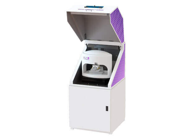
G200X Semi Pack

The G200X Semi Pack is a comprehensive test package designed to help improve yields and reduce latent defects for semiconductor and compound semiconductor films. The Semi Pack includes a wafer tilt chuck, AccuFilm™ Ultra Method Pack, Adhesion Method Pack, Thin Film Scratch Method Pack, Analytical Scanning Probe Microscopy, and automated routines for testing, image capture and survey scanning.

300°C Sample Heating

The 300°C sample heating option allows the sample to be placed into a chamber for uniform heating while simultaneously undergoing tests with either the InForce 1000 or InForce 50 actuators. The option includes high-precision temperature control, inert gas backfill to reduce oxidation, and cooling to remove waste heat. ProbeDMA, AccuFilm, NanoBlitz and CSM are all compatible with the sample heating option.
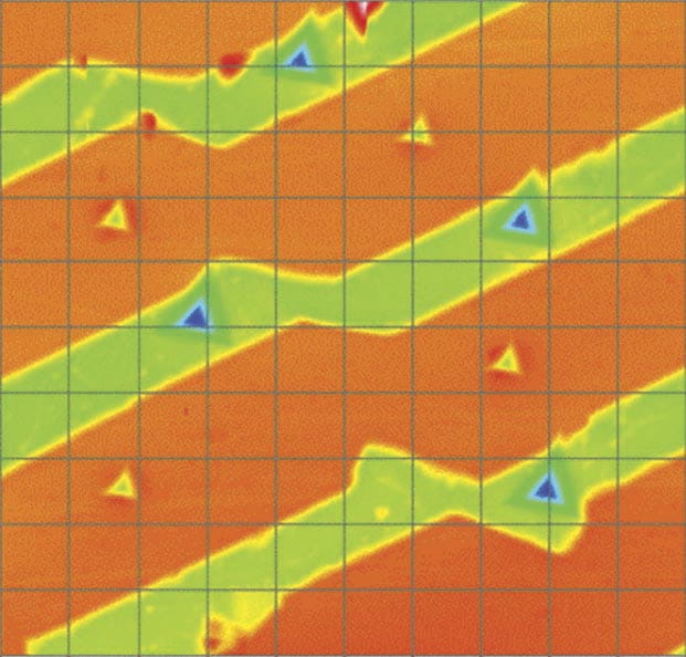
NanoBlitz 3D

NanoBlitz 3D utilizes the InForce 50 or InForce 1000 actuator and a Berkovich tip to generate 3D maps of nanomechanical properties for high-E (> 3GPa) materials. NanoBlitz performs up to 90,000 indents (300×300 array) at < 1s per indent, and provides Young’s modulus (E), hardness (H), and stiffness (S) values at a specified load for each indent in the array. The large number of tests enables increased statistical accuracy. Histogram charts show multiple phases or materials. The NanoBlitz 3D package includes visualization and data handling capabilities.

NanoBlitz 4D

NanoBlitz 4D utilizes the InForce 50 or InForce 1000 actuator and a Berkovich tip to generate 4D maps of nanomechanical properties for both low-E/H and high-E (> 3GPa) materials. NanoBlitz performs up to 10,000 indents (100×100 array) at 5-10s per indent, and provides Young’s modulus (E), hardness (H), and stiffness (S) values as a function of depth for each indent in the array. NanoBlitz 4D utilizes a constant strain rate method. The package includes visualization and data handling capabilities.

AccuFilm™ Thin Film Method Pack

The AccuFilm Thin Film Method Pack is an InView test method based on the Hay-Crawford model for measuring substrate-independent material properties using Continuous Stiffness Measurement (CSM). AccuFilm corrects for substrate influence on film measurements for hard films on soft substrates, as well as for soft films on hard substrates.
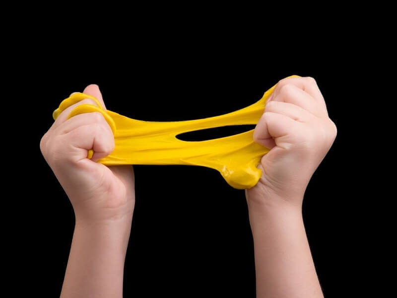
ProbeDMA™ Polymer Method Pack

The Polymer Pack provides the ability to measure the complex modulus of polymers as a function of frequency. The pack includes a flat-punch tip, a viscoelastic reference material, and a test method for evaluation of viscoelastic properties. This measurement technique is key to characterizing nanoscale polymers and polymer films that are not well-served by traditional dynamic mechanical analysis (DMA) test instruments.

Biomaterials Method Pack

The Biomaterials Method Pack provides the ability to measure the complex modulus of biomaterials with shear moduli on the order of 1kPa, and utilizes Continuous Stiffness Measurement (CSM). The pack includes a flat-punch tip and a test method for evaluation of viscoelastic properties. This measurement technique is key to characterizing small scale biomaterials that are not well-served by traditional rheometer instruments.
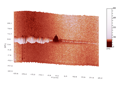
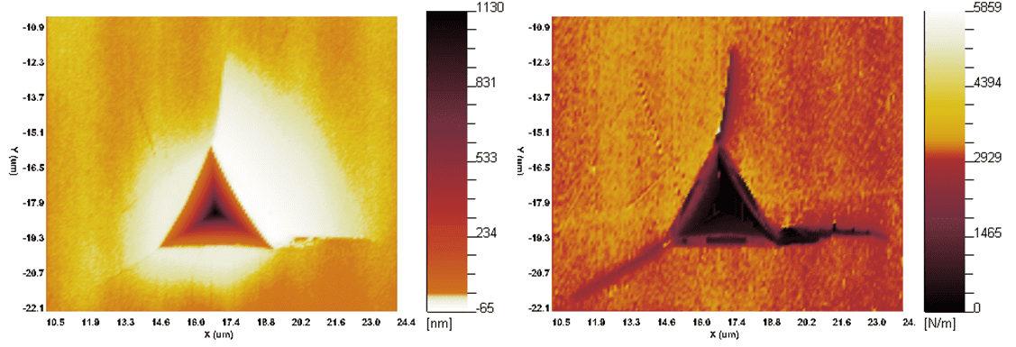
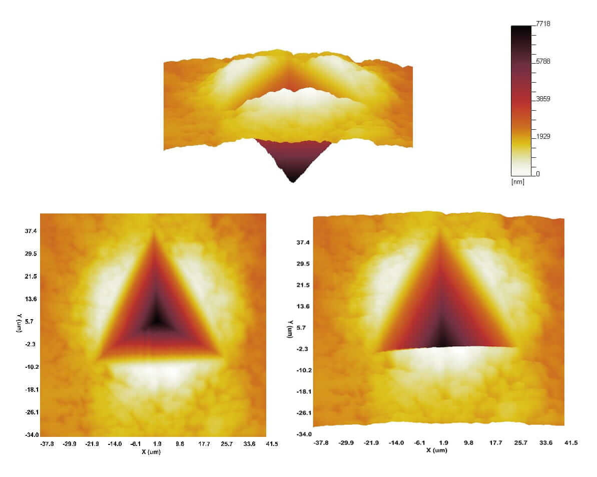
NanoVision

The NanoVision option features a closed loop nanopositioning stage for high-resolution 3D imaging and precise targeting. NanoVision allows users to target indentation test sites with nanometer-scale precision and characterize individual phases of complex materials. NanoVision users can also examine residual impressions to quantify material response phenomena such as pile-up, deformed volume and fracture toughness.
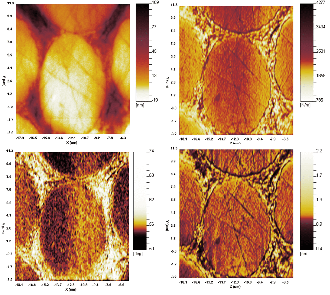
 

Survey Scanning

The Survey Scanning option utilizes the accurate, repeatable X/Y motion of the Nano Indenter G200X system to provide a maximum scan size of 500μm by 500μm. 10nm linear encoders provide improved imaging over the G200. The NanoVision stage and Survey Scanning options can be used together for precise location targeting for nanoindentation tests, particularly valuable for determination of sample fracture toughness.
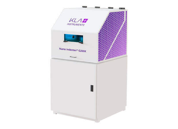
InView Software Versions

All Nano Indenter G200X systems are powered by the standard InView software. NanoSuite® Professional version gives users access to pre-written test methods, including methods that comply with ISO 14577 standards. The InView Method Development option enables researchers to write their own InView test methods using a simple protocol. The InView software suite includes InView ReviewData and InFocus applications that make reviewing data and creating presentations easy. InView features a Simulation Mode so that users can write test methods, process and analyze data offline.

Coating Hardness and Modulus Measurements (Oliver-Pharr)

Mechanical characterization is critical in the process and manufacture of films, including the quality of coatings in the automotive industry, as well as during process control of front-end and back-end semiconductor manufacturing. The G200X nanoindenter is capable of measuring hardness and modulus for a wide variety of materials, from ultra-soft gels to hard coatings. The high speed assessment of these properties enables quality control and assurance on production lines.

High Speed Material Property Maps

For many materials, including composites, the mechanical properties may vary widely from one area to the next. The G200X system provides a sample stage movement of 100mm in the X and Y axes, and 25mm in the Z axis, allowing testing of a wide range of sample heights over a large sample area. The optional NanoBlitz Topography and Tomography software can quickly generate color maps of any of the measured mechanical properties.

Yield stress/strain

The Nano Indenter G200X includes a pre-written ISO 14577 test method that measures material hardness in compliance with the ISO 14577 standard. This test method automatically measures and reports Young’s modulus, instrumented hardness, Vickers hardness and the normalized work-of-indentation.

Interfacial adhesion measurement

Thin film delamination is generally induced by depositing a highly compressive layer that can store elastic energy. The interfacial adhesion measurement is critical to assist users in understanding the failure mode of the thin film. Nano Indenter G200X systems can initiate the interfacial fracture and measure the adhesion and residual stress properties of the multiple-layer thin film.

Fracture Toughness

Fracture toughness is the critical value of the stress-intensity factor at which catastrophic failure occurs under plane-strain conditions. Lower values of fracture toughness indicate a pre-existing flaw. Evaluating fracture toughness by nanoindentation is accomplished easily by using the Stiffness Mapping method. (Stiffness mapping requires the Continuous Stiffness Measurement and NanoVision options.)

Viscoelastic Properties

Polymers are exceptionally complex materials; their mechanical properties depend on chemistry, processing and thermo-mechanical history. Specifically, the mechanical properties depend on the type and length of the parent chain, branching, cross-linking, strain, temperature, and frequency, and these dependencies are generally interrelated. In order to gain useful information for making decisions when designing with polymers, mechanical property measurements should be made on a relevant sample in a relevant context. Nanoindentation testing makes such context-specific measurements more accessible, because samples can be small and minimally prepared. The Nano Indenter G200X system can also be used to measure complex modulus and the viscoelastic properties of the polymer by oscillating the indenter while in contact with the materials.

Scanning Probe Microscopy (3D Imaging)

The Nano Indenter G200X system provides two scanning probe microscopy methods to characterize the crack length of indentation impression for measurement of fracture toughness in design applications. Fracture toughness is defined as the ability of a defective material containing a crack to resist fracture. The piezo stage of the Nano Indenter G200X, with its high positioning accuracy combined with the NanoVision option, provides up to 1nm encoder resolution of step size with a maximum 100µm by 100µm scan size. The Survey Scanning software option combines the X/Y motion system with InView software to provide a maximum scan size of 500µm by 500µm. Both the NanoVision stage and Survey Scanning option are required to target precise areas of samples for nanoindentation testing and calculation of fracture toughness.

Quantitative scratch and wear testing

The G200X system can perform scratch and wear testing on a variety of materials. Coatings and films are subjected to many processes that test the strength of these films and their adhesion to the substrate, such as chemical-mechanical polishing (CMP) and wire bonding. It is important for these materials to resist plastic deformation during these processes, and to remain intact without blistering up from the substrate. Ideally, a dielectric material will have a high hardness and elastic modulus because these parameters help define how the material will react when subjected to manufacturing processes.

High temperature nanoindentation testing

Nanoindentation at elevated temperatures is critical to characterizing material performance under thermal stress, especially for quantifying failure mechanisms during thermomechanical processing. Varying the sample temperature during mechanical testing enables not only measurement of thermal-induced behavioral changes, but also quantification of transition plasticity of materials that are not easily tested on the nano-scale.

related news

contact us

我们希望了解您的需求,请填写以下表单并提交

Your Name
邮箱地址
联系电话
您的需求