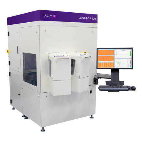
Candela® 8520 Surface Defect Inspection System
The Candela 8520 second generation integrated photoluminescence (PL) and surface inspection system is designed for advanced characterization of substrate and epitaxial defects on SiC and GaN substrates. Applications include GaN inspection with capability to detect crystal dislocation defects. Implementation of automated wafer inspection with statistical process control (SPC) methodology significantly cuts yield loss due to epi defects, minimizes metal-organic chemical vapor deposition (MOCVD) reactor process excursions, and increases MOCVD reactor uptime.
The Candela 8520 surface inspection system employs proprietary optical technology to simultaneously measure scatter intensity at two angles of incidence. It captures topographic variations, surface reflectance, phase shift and photoluminescence for automatic detection and classification of a broad range of defects of interest (DOI). The 8520 provides surface and photoluminescence defect inspection for GaN wafers, detecting and classifying GaN dislocations, pits and holes for GaN reactor defect control. Its power applications include SiC based transparent wafer inspection and classification of crystal defects such as BPDs (Basal Plane Dislocations), micropipes, stacking faults, bar stacking faults, grain boundaries, and threading dislocations. Detection of topographic anomalies include triangle detection, carrot defects, downfall and scratches.