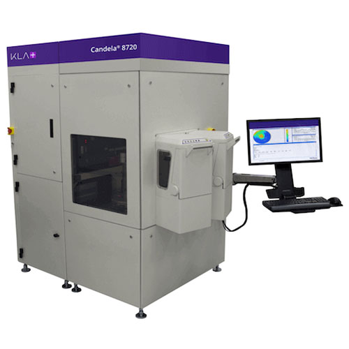
Candela® 8720 Surface Defect Inspection System
The Candela 8720 advanced integrated surface defect inspection and photoluminescence (PL) defect inspection system captures a variety of mission-critical substrate and epitaxial defects. Implementation of automated wafer inspection with statistical process control (SPC) methodology significantly cuts yield loss due to epi defects, minimizes metal-organic chemical vapor deposition (MOCVD) reactor process excursions, and increases MOCVD reactor uptime.
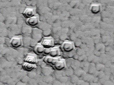
The Candela 8720 wafer inspection system employs proprietary optical technology to simultaneously measure scatter intensity at two angles of incidence. It captures topographic variations, surface reflectivity, phase shift and photoluminescence for automatic detection and classification of a broad range of defects of interest (DOI). Applications of advanced surface inspection include GaN inspection for radio frequency (RF), power and high brightness light emitting diode (HBLED), with capability to detect cracks, crystal dislocation defects, hillocks, micropits, sliplines, bumps and hex bumps, and epi defects. The 8720 inspection system is also used for defect inspection on other high-end compound semiconductor process materials such as Gallium Arsenide (GaAs) and Indium Phosphide (InP) for LED, VCSELs and photonics applications.