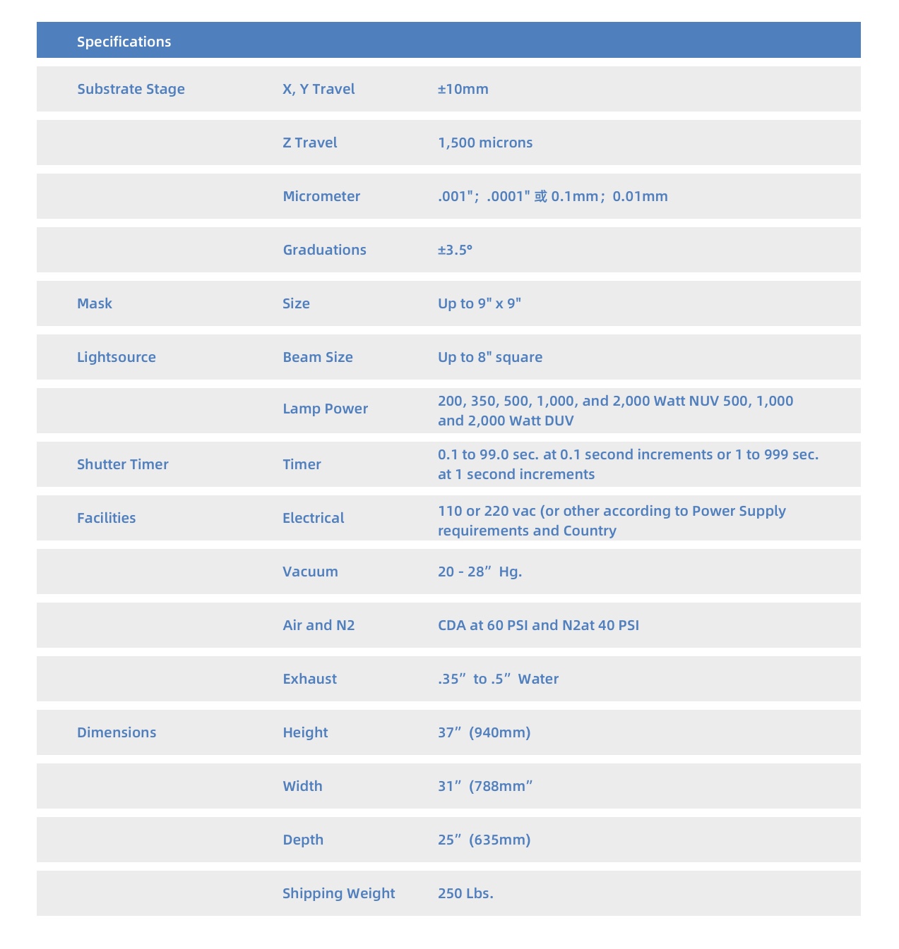
Model 200 Mask Alignerand UV Exposure System
The OAI Model 200 Mask Aligner and UV Exposure System is a cost-effective high performance
tool that is engineered with the industry proven modular components that make OAI a leader
in the MEMS, Nanotechnology and Semiconductor equipment industries. The Model 200 is a
bench top model that requires minimal clean room space. It offers an economic alternative for
R&D, pilot, or low volume production. Utilizing an innovative, air bearing / vacuum chuck leveling
system, the substrate is leveled quickly and gently for parallel photomask alignment and uniform
contact across the wafer during contact exposure. The system is capable of micron resolution and
alignment precision. The Alignment Module features mask insert sets and quick-change wafer
chucks that allow the use of a variety of substrates and masks without requiring tools for
reconfiguration. The Alignment Module incorporates micrometers for the X, Y, and θ axes. The
Model 200 Aligner can be fitted with a wide range of alignment optics including backside IR. The
IR illumination vacuum chuck can be configured for alignment of whole wafers or pieces. The
OAI Model 200 can be configured with an OAI Nano Imprint Module making it the lowest cost
NIL tool available. OAI also offers a module designed for using liquid photoploymers for rapid
prototyping or production of microfluidic devices.
The Model 200 features a dependable OAI light source that provides collimated UV light
in Near or Deep UV using lamps ranging in power from 200 to 2000 watts. Dual-sensor,
optical feedback loops are linked to the
Constant Intensity Controller to provide
control of exposure intensity within ±2% of
the desired intensity. Changes may be made
to the UV wavelength quickly and easily.
———————————————————————————————
Applications:
MEMS
NIL
Microfluidics
Nanotechnology
II-VI & III-V device fabrication
Multi-level resist processing
LCD and FED displays
MCM’s
Thin film devices
Solar cells
SAW devices
Options
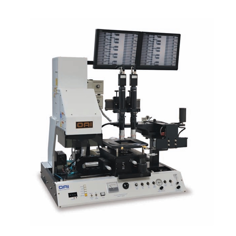
Available with single or dual
cameras and screens
(Dual camera / dual screen version
shown in photo)
May be fitted with Nano Imprint
Module for NIL
May be fitted with Module for
Microfluidics
Features
Small Footprint
Vacuum Chuck
Precision Alignment Module
Interchangeable Mask Holders
and Substrate Chucks
Benefits
Requires minimal clean
room space
■ Causes minimal damage to
fragile substrate materials
■ Accurate alignments
to 1 micron
■ Easily accommodates a
wide variety of substrates
and masks
■ Backside mask alignment
of IR transparent wafers
with accuracy up to 3-5
microns
■ Highly collimated, uniform
UV light
■ Quickly change the UV
light wavelength
■ Exposure controlled
intensity to ±2%
■ Can be configured as a
Nano Imprint tool for NIL
■ Can be configured with a
Microfluidics Module