ezSTM | Scanning Tunneling Microscope
Compact Scanning Tunneling Micrscopy
Scanning Tunneling Microscope is a device to scan conductive sample surfaces at the atomic scale. Quantum tunneling leads the STM theory. Conductive tip reaches to the conductive sample surface with a bias Voltage, and electrons can be tunneled between the sample and tip. As a result of this, tunnel current is occurred.
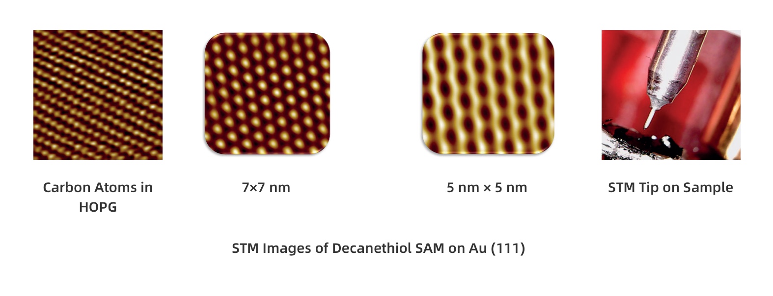
The ezSTM is a compact Scanning Tunneling Microscope System which provides excellent performance through all of these steps above. Besides its high performance, it is remarkably affordable as well. ezSTM is ideal for student laboratories, high schools, nanotechnology educations and basic researches with its compact, high stability and user-friendly design. ezSTM can be setup in 5 minutes, and after installation you are ready to explore atoms in minutes with ezSTM. Atomic resolution is obtained by ezSTM with high performance.
All ezSTM components which is controller, ezSTM scanner head, vibration isolation apparatus and laptop are included inside of the small suitcase. From the beginning, power cable, 2 USB cables and head cable are plugged and the user-friendly software is opened to start measurements. All of the software installation process are made by the ezSTM-Application Scientists of Nanomagnetics Instruments. After installation, you are ready to take measurements at an atomic resolution with the easy use of software interface.
ezSTM Design
The flexible design of the ezSTM allows to replace/move the scan head easily, and it provides easy usage for customers with the small footprint by an ultimate performance. Because the ezSTM takes a small space, and does not heavy, it can be transport easily.
Pt/Ir wire which is more simple and harmless than tip etching by dangerous chemicals is cut as a tip for scanning, and tip replacement is very simple which makes the ezSTM user-friendly. NanoMagnetics Instruments provides Pt/Ir wire in the ezSTM system User Kit for the customers.
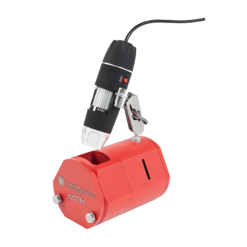
Side view camera is located on the ezSTM scanner head, and it is useful to observe the sample, tip and the movement. The movement is done by ultrasonic motors. Also, maximum scan area of the ezSTM is 1x1x0.5 um. After all steps, you will be able to scan at the atomic resolution for your samples.
-
1pA-10nA or 100pA-100nA current range
-
0.1pA current step size
-
0.5x0.5x0.2μm or 1x1x0.5μm(XYZ)Scanner
-
Z resolution 0.5pm
-
XY resolution 1pm
-
Constant current,constant height imaging modes
-
Curren-Voltage,Current-Distance spectroscopy
-
Tip voltage±15V in 300μV steps
-
Ultrasonic motors for fastest sample approach &XY
coarse sample positioning up to 5mm
-
Sample thickness up to 15mm
-
2MP CMOS,LED illuminated side view video camera
with manual focusing and 5X digital zooming
-
Digital Feedback: Equipped with Field-Programmable Gate Array/Digital Signal Processor (FPGA/DSP)
-
Analog-to-Digital (A/D) / Digital-to-Analog (D/A) Converters: 24 Bits
-
Simultaneous scan of 6 channels @
4096x4096 pixels
-
Interface: USB
-
100-240 VAC,50/60Hz,50W