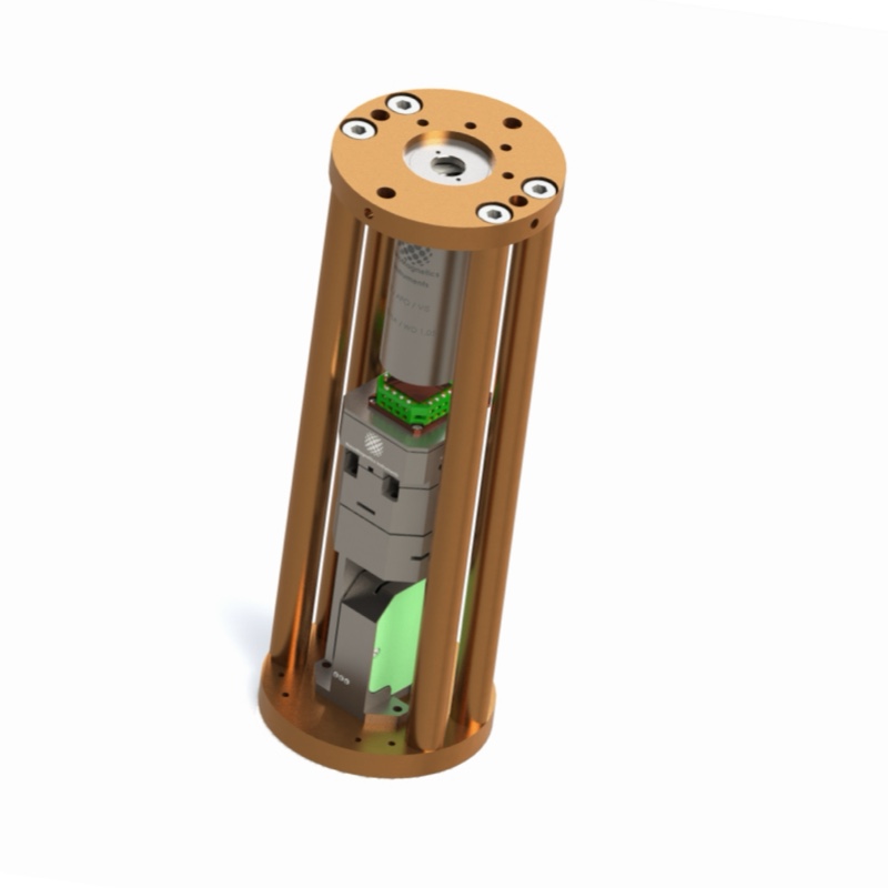
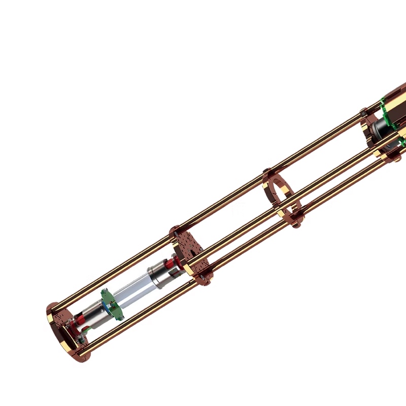
Specifications
0.82 NA / 0.95mm WD Low Temperature APO Objective
10mK-300K Temperature Range
Magnetic Fields Up to 31 Tesla
System Specifications
-
Scan range: 50x50x25μm @ 300K / 30x30x15μm @4K
-
Sample Approach: 6x6x12mm XYZ range with 50 - 700nm step size
-
Closed Loop Operation: Resistive encoder with 200nm resolution
-
Fine Scanning Range: 7.5μm @300K / 1μm @4.2K
-
Sample Size:10x10x5mm maximum
-
8 pin connections for experiments
-
Temperature Range:10mK-300K(Limited by the system)
-
Magnetic Field: up to 31T
-
Operation:Vacuum or exchange gas environment
-
Compatibility: Compatible with most cryostats & Dilution Refrigerators with 50mm Cold bore
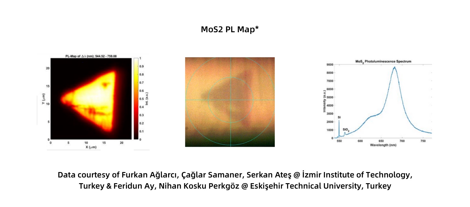
It covers parameters such as scanning, sample adaptability, environmental control, and compatibility, and is used in special experimental scenarios including low-temperature and high-magnetic-field conditions (e.g., quantum materials research).
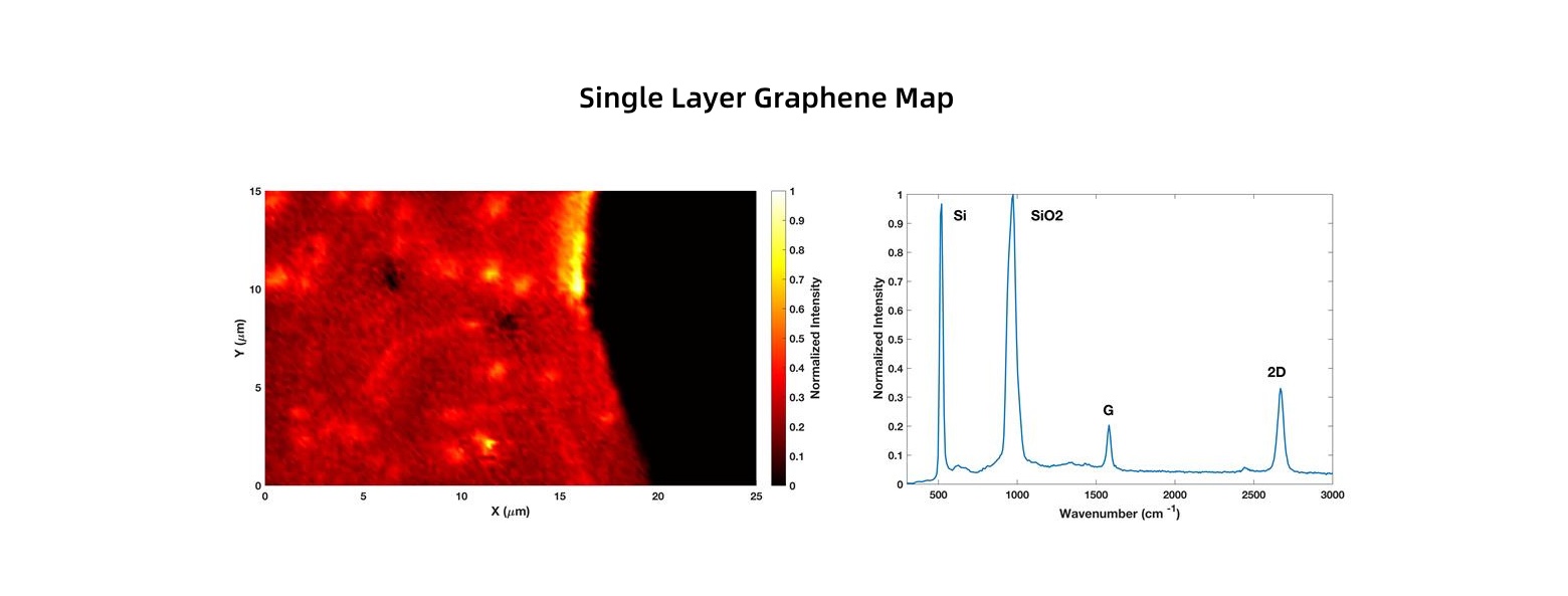
In the fields of materials science, nanotechnology, and others, it often refers to images that capture the spatial distribution of the properties (structural, optical, electrical, etc.) of single-layer graphene. These images are obtained through specific characterization techniques (such as Raman mapping, scanning probe microscopy, etc.) and are used to study the uniformity, defects, and other characteristics of single-layer graphene.